

KOR Request a Quote
Researcher holding a semiconductor chip EV battery platform
Optical Precision Measurement · Inspection Solutions

Revealing invisible
differences in numbers

Inspection and measurement solutions for the display, semiconductor, secondary battery, industrial materials and bio industries. From thin film thickness and sheet resistance to spectroscopy and hyperspectral imaging, we propose the right equipment for your process.

Request Sample Measurement View all products

Products

Find equipment by what you want to measure. Each product page offers specifications and catalogs.

Not sure which equipment fits? →
Thin Film Thickness Gauge
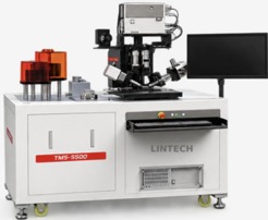
Ellipsometer (SE) & Reflectometer (SR) Measures thin film thickness and refractive index (n&k) optically without contact in under 1 second. From manual lab units to automated stages, fully automatic SE+SR and inline semiconductor CMP systems, for display, power semiconductor, battery and film materials.
ST-1000 ST-2000 ST-4000 ST-5030 SE+SR ILTHK-1000
Hyperspectral Camera
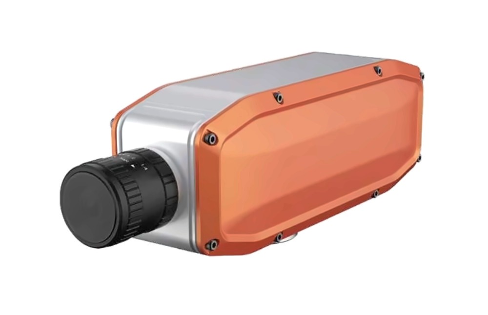
Hyperspectral Imaging Camera 10 product families: portable, line-scan, high-speed industrial SWIR (up to 7800 fps), imaging, microscope, PTZ · SIF, drone-mounted, multispectral and solar EL/PL inspectors. Covers 300–2500 nm.
Line Scan FS-1X Industrial FS-19S Imaging FS2X Portable FS-IQ Microscope FS-MS UAV FS60-CL
Spectrometer
Spectrometer
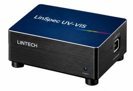
LINSPEC Spectrometer Series 15 models in 7 families, from miniature UV-VIS to high resolution (down to 0.06 nm), area array, TE-cooled and NIR (up to 2500 nm). Wavelength range and resolution can be customized.
Miniature UV-VIS High Resolution Area Array TE-Cooling NIR NIR TE-Cooling
Scanning Electron Microscope
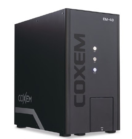
Scanning Electron Microscope (SEM) · COXEM From the EM-40 tabletop SEM to the CX-200K with up to 500,000× and the CX-300 for large-area analysis. Sample preparation equipment such as ion sputter coaters and ion beam polishers is also supplied.
EM-40 EM-30N CX-200K CX-300 SPT-20 IP-10K
Optical Microscope
Optical Microscope
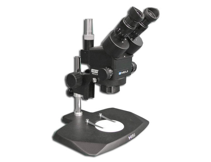
Optical Microscope · Meiji Techno (Japan) We supply stereo zoom microscopes (7X–90X), SMT boom stand inspection systems, upright and inverted metallurgical microscopes and 4K microscope cameras from Meiji Techno, Japan. From electronic component inspection to metallographic analysis.
EMZ-8TR SMT-8TR MT8530M IM7200M HD4000K-M
Optical Components
Optical Components
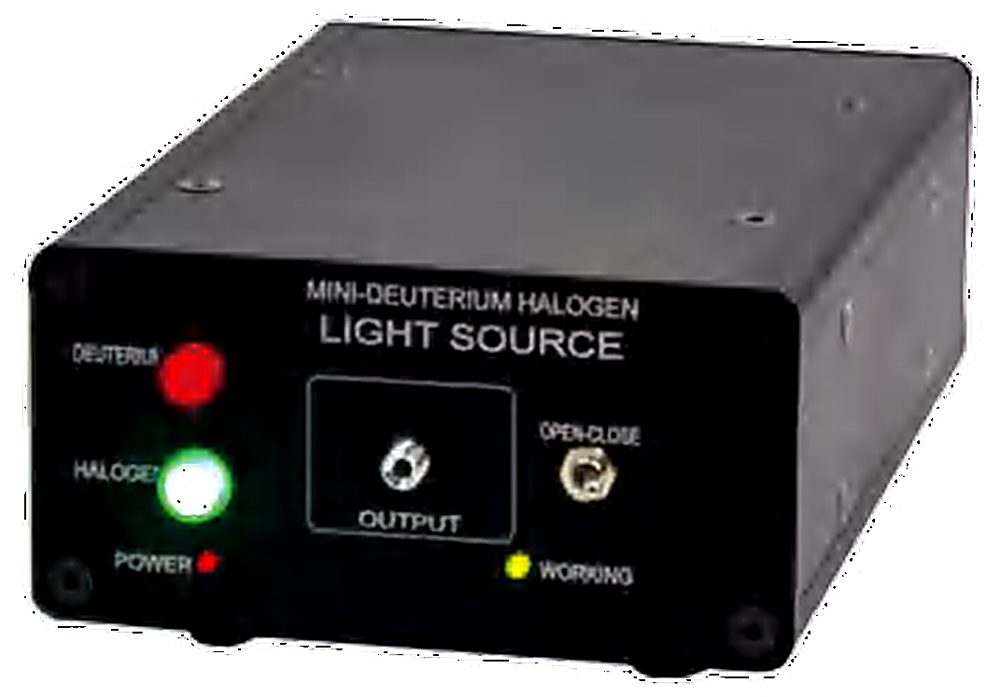
Light Source & Optical Fiber We supply tungsten, deuterium-halogen, LED and mercury calibration light sources for spectroscopy, along with custom optical fibers (1-to-1, Y-type).
Tungsten Light Source Deuterium-Halogen Light Source LED Light Source Mercury calibration light source Optical Fiber
Sheet Resistance Meter
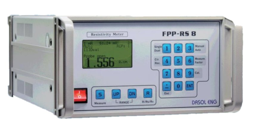
Desk Top Type Resistivity Meter · 4-Point Probe Measures sheet resistance (1 mΩ/sq – 1 GΩ/sq), resistivity and resistance of thin films by 4-point contact. Select Single · Dual · Bulk modes with instant unit conversion.
RSD-1G RSD-40k
Wafer Thickness Measurement
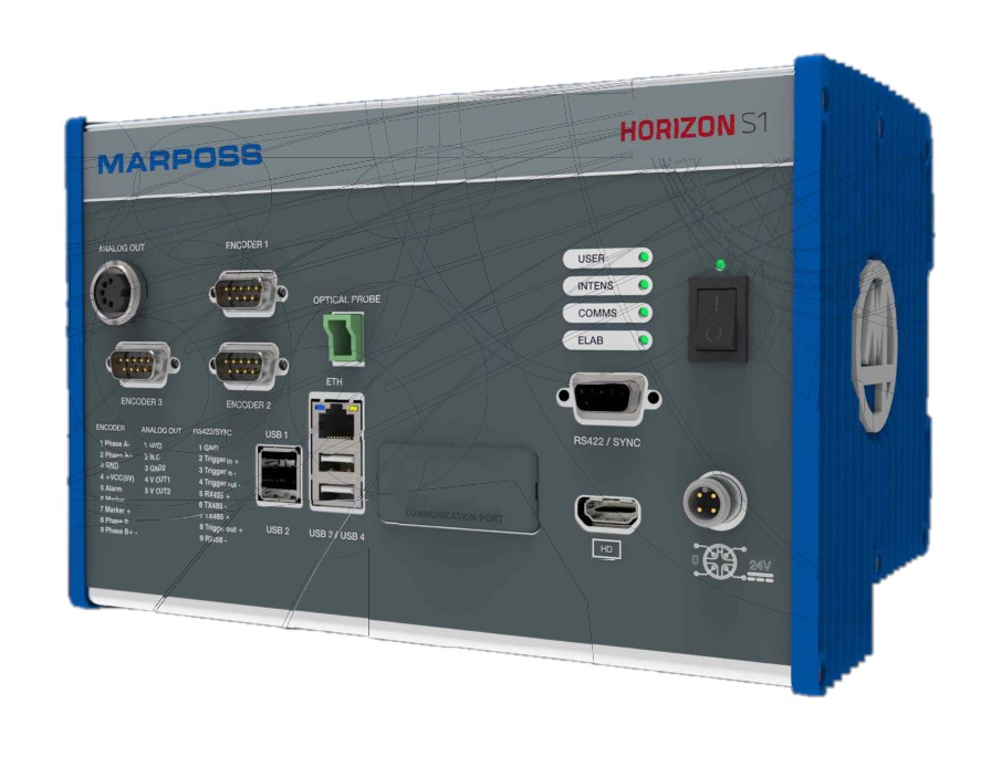
Wafer Thickness Measurement · Marposs HORIZON Non-contact measurement of thickness and warpage of silicon, SiC and GaN wafers and thin films by interferometry. 30 nm axial resolution and up to 90 kHz sampling support in-process measurement during back-grinding.
HORIZON S1 / 90S1 S2 / 90S2 T1 / 90T1 W1 L2

Equipment we
proudly recommend

Our most requested equipment, whose performance we can show right away with sample measurements.

Hyperspectral Camera
Hyperspectral Camera 10 product families, from line-scan to drone-mounted Learn more →
Thin Film Thickness Gauge
Thin Film Thickness Gauge 6 models, from manual to CMP inline Learn more →
LINSPEC spectrometer
LINSPEC spectrometer 15 models, from miniature to NIR TE-cooled Learn more →

Applications

Choose an industry to see the measurement equipment mainly used in that field.

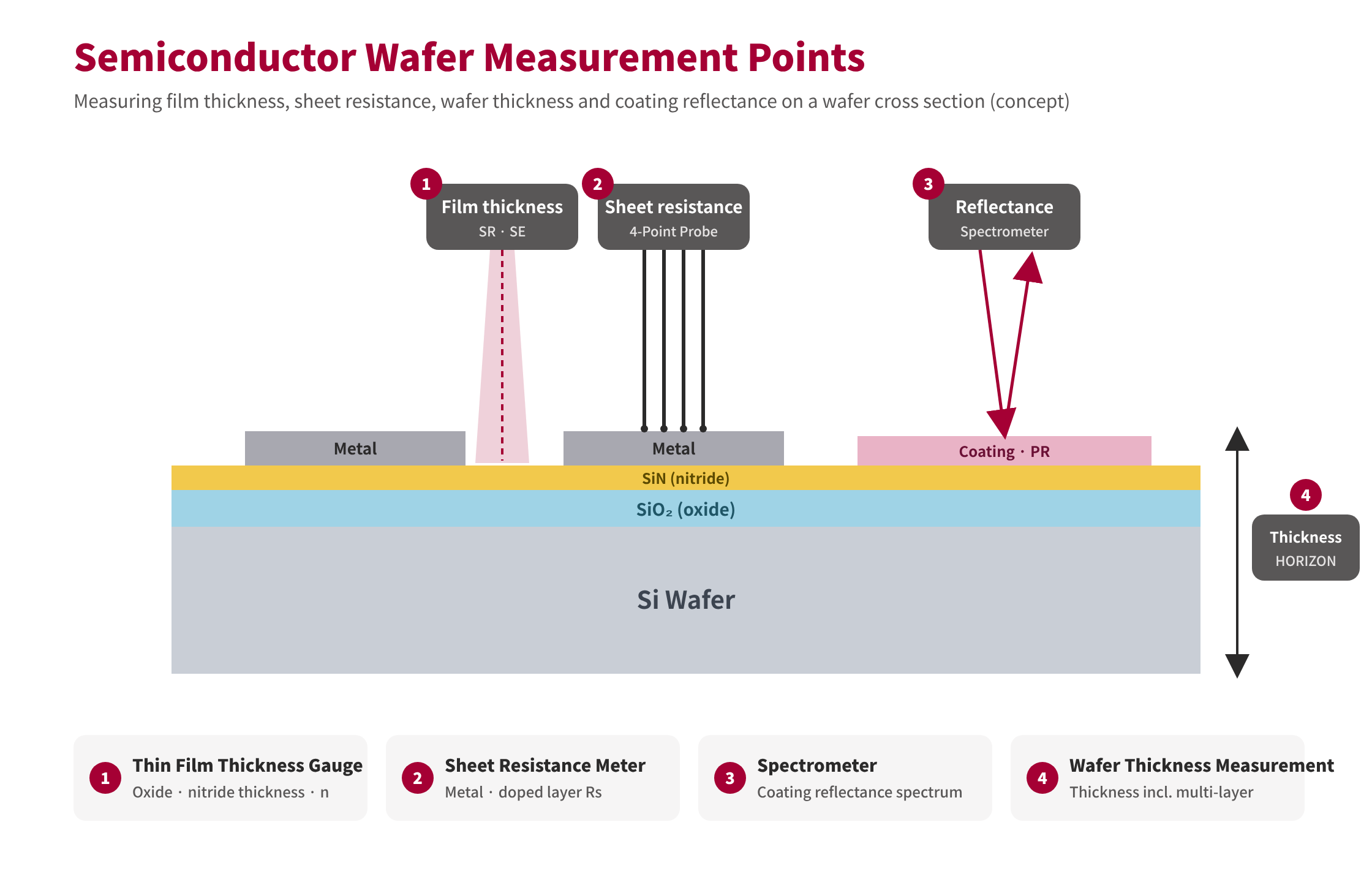
Semiconductor wafer measurement points
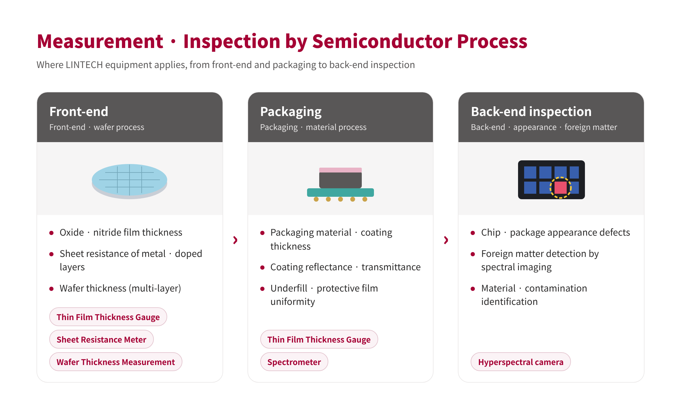
Measurement · inspection by semiconductor process

Semiconductor

For front-end and packaging material thickness, sheet resistance, wafer coating reflectance and back-end inspection.

Thin Film Thickness Gauge Sheet Resistance Meter Wafer Thickness Measurement Hyperspectral Camera

Through constant progress,
we aim to be a global leader
in our market

LINTECH is a specialist developing inspection and measurement solutions for the display, semiconductor, industrial materials and secondary battery industries.

Hello, this is LINTECH. Founded in 2022, LINTECH is recognized for its technology and quality. From thin film thickness gauges, hyperspectral cameras and spectrometers to sheet resistance meters and optical components, we work with many companies and strive to be a trusted partner.

We will keep earning your trust and continue to grow so you can rely on us. Thank you.

Hyunmok Kwon, CEO, LINTECH

Philosophy 01

Technology Innovation

We believe new technology drives company growth, and we continuously innovate.

Philosophy 02

Best Quality

Our engineers and researchers work continuously to deliver the best products and service quality.

Philosophy 03

Trust Management

Trust is our name. We take responsibility and do our best.

Patents

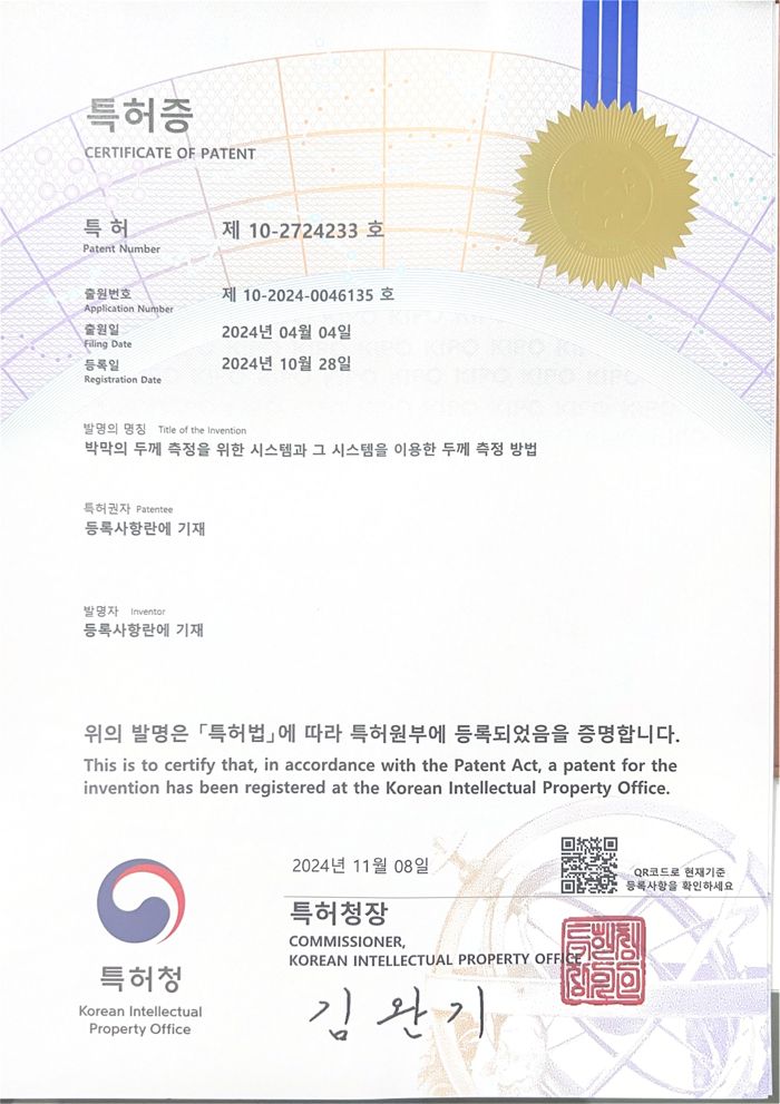
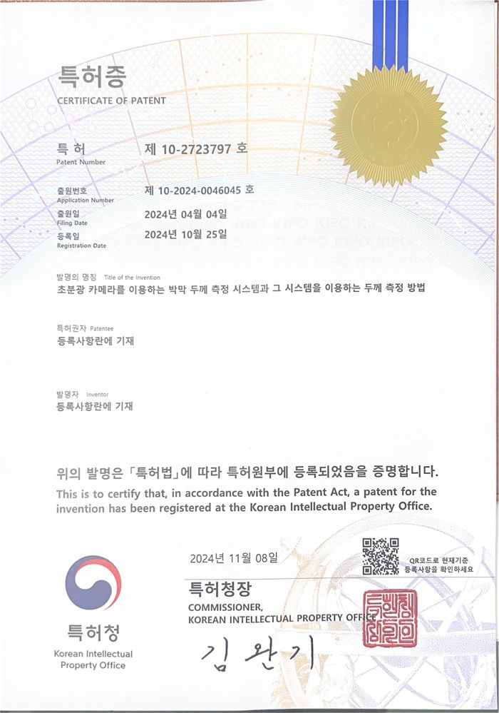
We hold two registered patents on thin film thickness measurement technology.
Patent certificate No. 10-2724233
Patent No. 10-2724233System for measuring thin film thickness and thickness measurement method using the systemFiled 2024.04.04 · Registered 2024.10.28
Patent certificate No. 10-2723797
Patent No. 10-2723797Thin film thickness measurement system using a hyperspectral camera and thickness measurement method using the systemFiled 2024.04.04 · Registered 2024.10.25

History

2026Selected for the KAIST Fast Prototyping ProgramKAIST Startup Center
2025Selected for the 2025 Commercialization Support ProgramHannam University Business Incubator
2025Selected for the Market Development Stepping Stone ProgramHannam University Business Incubator
2024. 102 patents registeredThin film thickness measurement system · thin film thickness measurement system using a hyperspectral camera
2023Selected for the Business Advancement ProgramDaejeon Center for Creative Economy & Innovation
2023. 07Selected for the Daejeon D-Bridge Startup Open Space ProgramDaejeon Center for Creative Economy & Innovation
2022. 12LINTECH founded

We measure before you buy

Some things cannot be learned from a spec sheet alone. LINTECH verifies results with your own samples before making a proposal.

STEP 01

Consultation

We check the target, parameters, precision and installation environment.

STEP 02

Sample Measurement

We measure your samples to verify suitability.

STEP 03

Custom proposal

We provide equipment configuration and a quote based on the results.

STEP 04

Installation · Training · Service

We handle on-site installation, user training and ongoing technical support.

Key Customers

Semiconductor · Display Industry
Samsung Electro-Mechanics Samsung SDI
KCTech SK Powertech LB Semicon
LG Chem Sunic System Duksan Neolux
Universities · Public Research Institutes
Seoul National University Yonsei University Hanyang University
Sungkyunkwan University POSTECH Korea University
KETI ETRI National NanoFab Center
Equipment · Materials · New Industries
LG Electronics
Egtech

Customer Support Center

One call covers equipment selection, quotes, operation and after-sales service.

Weekdays 09:00 – 18:00 (KST) 042-361-9999
Kakao Map will be displayed here
Location410-2, Innobiz Park, Hannam University Daedeok Valley Campus, 1646 Yuseong-daero, Yuseong-gu, Daejeon, Korea

Downloads

Download product catalogs, spec sheets and application notes.

Go to downloads →

Just send us your samples.
We will answer with measurement results.

Tell us what you measure, the values you need, the required precision and the installation environment (lab or production line), and we will contact you quickly.

T. 042-361-9999 E. lin-tech@lin-tech.co.kr
Quick Consult