Ellipsometer (SE) & Reflectometer (SR)
Thin Film Thickness Gauge
Find new value with the light
Measures the thickness and refractive index (n&k) of transparent, opaque, conductive and non-conductive thin films optically without contact in under 1 second. The lineup ranges from manual lab units to automated stage types and inline systems for semiconductor CMP.
Patent No. 10-2724233 · System for measuring thin film thickness and thickness measurement method using the system
A few Å – 35 µmMeasuring Range (SE + SR)
≤ 1 sMeasurement Speed
6Model
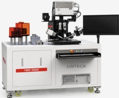
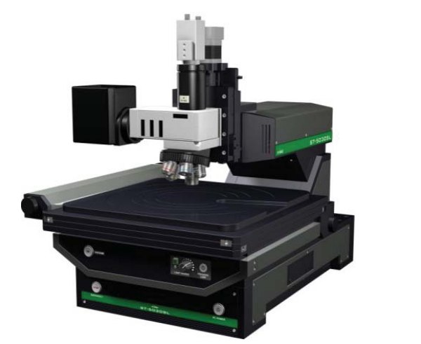
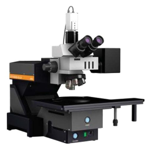
Product Lineup
Select a model to see photos, features and specifications.
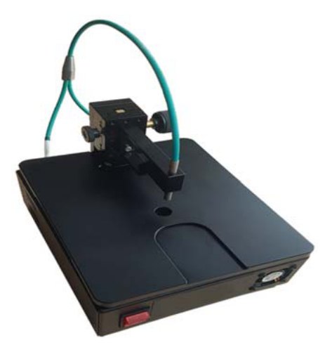
MANUAL · Universities · Institutes
ST-1000
Reflectometer (SR)
Samples of various sizes
Budget-focused model
Available as a module
Thickness of transparent, opaque, conductive and non-conductive films with various dispersion models
Under 1 second per measurement, simple operation and easy-to-use software
Thickness of display, power semiconductor and battery materials, materials and films
| Method | Manual Type |
|---|---|
| Sample Size | Up to 150 × 120 mm |
| Measurement Type | Non-contact optical |
| Measuring Range | VIS-NIR type: 500 Å – 35 µm UV-VIS type: 300 Å – 35 µm |
| Measurement Spot | 1 mm (Typical) |
| Measurement Light Source | VIS-NIR: Tungsten Halogen UV-VIS: Deuterium + Tungsten Halogen |
| Option | Certified thickness standard · UV thickness function · thick-film program (FFT) |
Model Comparison
SR : Spectroscopic Reflectometer · SE : Spectroscopic Ellipsometer| Model | ST-1000 | ST-2000 | ST-4000 | ST-5030 | SE+SR | ILTHK-1000 |
|---|---|---|---|---|---|---|
| Method | Manual | Manual | Manual | Automatic | Automatic (SE+SR) | Inline Automatic |
| Principle | SR | SR | SR | SR | SE + SR | SR + Vision |
| Sample Size | 150 × 120 mm | 210 × 140 mm | 200 × 200 mm | 300 × 300 mm | 300 × 300 mm | 300 × 300 mm |
| Measuring Range | 300 Å – 35 µm | 300 Å – 35 µm | 300 Å – 35 µm | 300 Å – 35 µm | A few Å – 35 µm | 300 Å – 35 µm |
| Measurement Spot | 1 mm | 20 µm | 20 µm | 20 µm | 20 µm / SE 150 × 300 µm or 30 × 60 µm | 20 µm |
| Recommended Use | Universities · Institutes | Corporate Labs | R&D · Production | Automatic multi-point measurement | Ultra-thin films · RI measurement | CMP process inline |
Measuring ranges depend on the film type. Common: non-contact optical measurement · transparent/opaque/conductive/non-conductive films · display · power semiconductor · secondary battery · materials/films
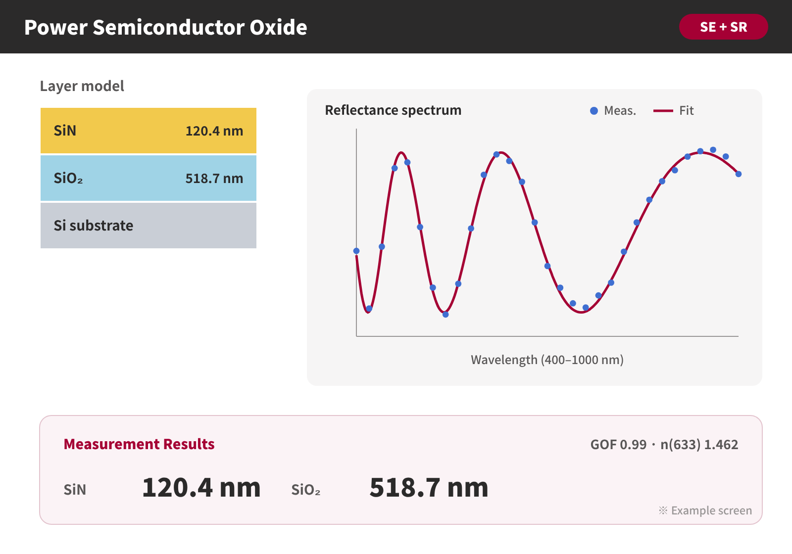
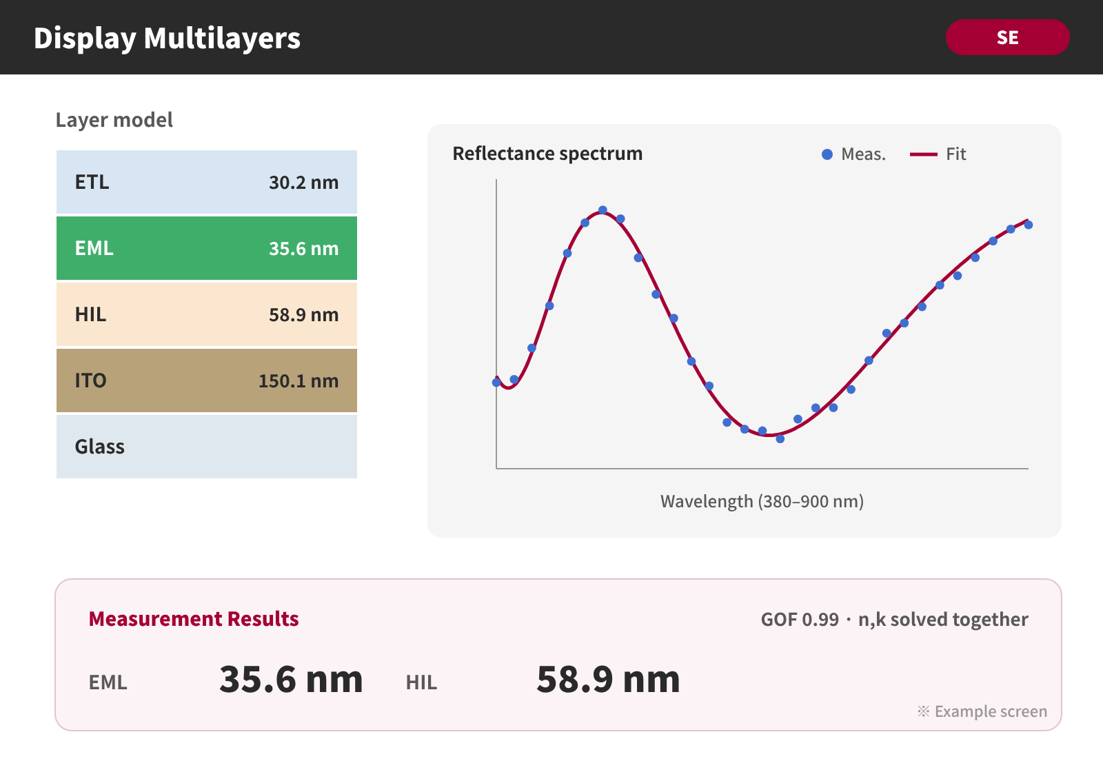
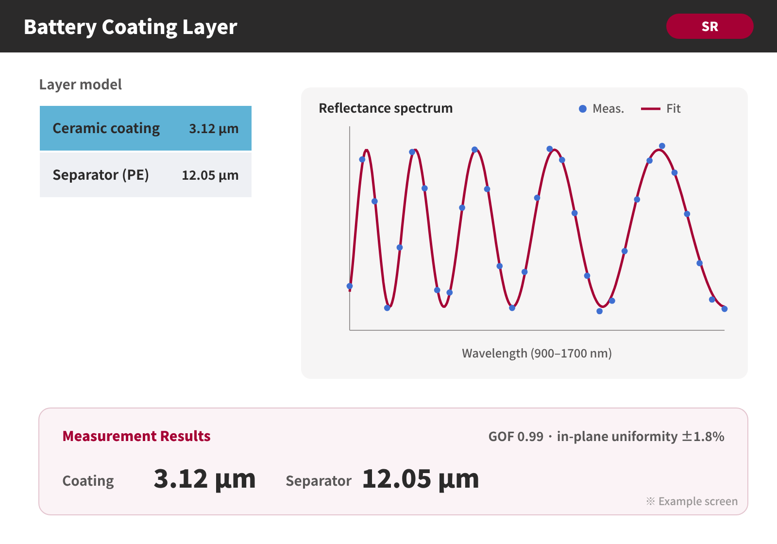
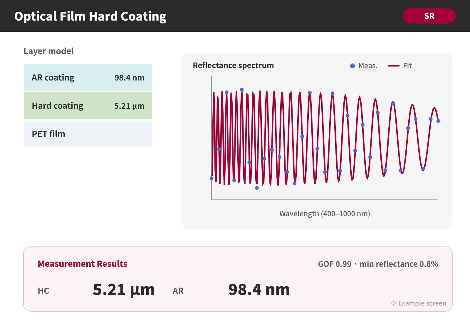
Measurement Examples
Thin film thickness results and analysis screens by material.